- 您现在的位置:买卖IC网 > Sheet目录395 > ATMEGA128RFA1-ZUR (Atmel)IC AVR MCU 2.4GHZ XCEIVER 64QFN
�� �
�
�ATmega128�
�AVR� CPU� Core�
�Introduction�
�Architectural�
�This� section� discusses� the� Atmel� ?� AVR� ?� core� architecture� in� general.� The� main� function� of� the�
�CPU� core� is� to� ensure� correct� program� execution.� The� CPU� must� therefore� be� able� to� access�
�memories,� perform� calculations,� control� peripherals� and� handle� interrupts.�
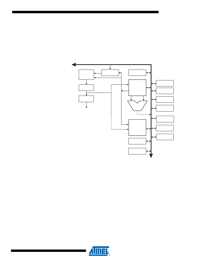
�Figure� 3.� Block� Diagram� of� the� AVR� Architecture�
�Overview�
�Data� Bus� 8-bit�
�Flash�
�Program�
�Memory�
�Program�
�Counter�
�Status�
�and� Control�
�Instruction�
�Register�
�32� x� 8�
�General�
�Purpose�
�Registrers�
�Interrupt�
�Unit�
�SPI�
�Unit�
�Instruction�
�Decoder�
�Control� Lines�
�ALU�
�Data�
�SRAM�
�W� atchdog�
�Timer�
�Analog�
�Comparator�
�I/O� Module1�
�I/O� Module� 2�
�I/O� Module� n�
�EEPROM�
�I/O� Lines�
�In� order� to� maximize� performance� and� parallelism,� the� AVR� uses� a� Harvard� architecture� –� with�
�separate� memories� and� buses� for� program� and� data.� Instructions� in� the� program� memory� are�
�executed� with� a� single� level� pipelining.� W� hile� one� instruction� is� being� executed,� the� next� instruc-�
�tion� is� pre-fetched� from� the� program� memory.� This� concept� enables� instructions� to� be� executed�
�in� every� clock� cycle.� The� program� memory� is� In-System� Reprogrammable� Flash� memory.�
�The� fast-access� Register� file� contains� 32� x� 8-bit� general� purpose� working� registers� with� a� single�
�clock� cycle� access� time.� This� allows� single-cycle� Arithmetic� Logic� Unit� (ALU)� operation.� In� a� typ-�
�ical� ALU� operation,� two� operands� are� output� from� the� Register� file,� the� operation� is� executed,�
�and� the� result� is� stored� back� in� the� Register� file� –� in� one� clock� cycle.�
�Six� of� the� 32� registers� can� be� used� as� three� 16-bit� indirect� address� register� pointers� for� Data�
�Space� addressing� –� enabling� efficient� address� calculations.� One� of� the� these� address� pointers�
�can� also� be� used� as� an� address� pointer� for� look� up� tables� in� Flash� Program� memory.� These�
�added� function� registers� are� the� 16-bit� X-register,� Y-register� and� Z-register,� described� later� in�
�this� section.�
�The� ALU� supports� arithmetic� and� logic� operations� between� registers� or� between� a� constant� and�
�a� register.� Single� register� operations� can� also� be� executed� in� the� ALU.� After� an� arithmetic� opera-�
�tion,� the� Status� Register� is� updated� to� reflect� information� about� the� result� of� the� operation.�
�9�
�2467X–AVR–06/11�
�发布紧急采购,3分钟左右您将得到回复。
相关PDF资料
ATMEGA64RZAPV-10AU
BUNDLE ATMEGA644P/AT86RF230 TQFP
ATP101-TL-H
MOSFET P-CH 30V 25A ATPAK
ATP102-TL-H
MOSFET P-CH 30V 40A ATPAK
ATP103-TL-H
MOSFET P-CH 30V 55A ATPAK
ATP104-TL-H
MOSFET P-CH 30V 75A ATPAK
ATP106-TL-H
MOSFET P-CH 40V 30A ATPAK
ATP107-TL-H
MOSFET P-CH 40V 50A ATPAK
ATP108-TL-H
MOSFET P-CH 40V 70A ATPAK
相关代理商/技术参数
ATMEGA128RFA1-ZUR SL514
制造商:Atmel Corporation 功能描述:
ATMEGA128RFA1-ZUR00
制造商:Atmel Corporation 功能描述:2.4GHZ 802.15.4 128K SOC REVF 制造商:Atmel Corporation 功能描述:2.4GHZ 802.15.4 128K SOC REVF T&R - Bulk 制造商:Atmel from Components Direct 功能描述:ATMEL ATMEGA128RFA1-ZUR00 MICROCONTROLLERS (MCU) 制造商:Atmel 功能描述:Atmel ATMEGA128RFA1-ZUR00 Microcontrollers (MCU) 制造商:Atmel Corporation 功能描述:MCU AVR 2.4GHZ 128K FLASH 64VQFN 制造商:Atmel Corporation 功能描述:2.4GHZ 802.15.4 128K SOC Revision F 制造商:Atmel 功能描述:2.4GHZ 802.15.4 128K SOC REVF
ATMEGA128RFR2-ZF
功能描述:IC RF TXRX+MCU 802.15.4 64-VFQFN 制造商:microchip technology 系列:- 包装:托盘 零件状态:在售 类型:TxRx + MCU 射频系列/标准:802.15.4 协议:Zigbee? 调制:DSSS, O-QPSK 频率:2.4GHz 数据速率(最大值):2Mbps 功率 - 输出:3.5dBm 灵敏度:-100dBm 存储容量:128kB 闪存,4kB EEPROM,16kB SRAM 串行接口:I2C,JTAG,SPI,USART GPIO:35 电压 - 电源:1.8 V ~ 3.6 V 电流 - 接收:5mA ~ 12.5mA 电流 - 传输:8mA ~ 14.5mA 工作温度:-40°C ~ 125°C 封装/外壳:64-VFQFN 裸露焊盘 标准包装:260
ATMEGA128RFR2-ZU
制造商:Atmel Corporation 功能描述:2.4GHZ 802.15.4 128K SOC IND 85C - Bulk
ATMEGA128RFR2-ZUR
制造商:Atmel Corporation 功能描述:2.4GHZ 802.15.4 128K SOC 85C T&R - Tape and Reel
ATMEGA128RZAV-8AU
功能描述:射频微控制器 - MCU AVR Z-Link Bundle RoHS:否 制造商:Silicon Labs 核心:8051 处理器系列:Si100x 数据总线宽度:8 bit 最大时钟频率:24 MHz 程序存储器大小:64 KB 数据 RAM 大小:4 KB 片上 ADC:Yes 工作电源电压:1.8 V to 3.6 V 工作温度范围:- 40 C to + 85 C 封装 / 箱体:LGA-42 安装风格:SMD/SMT 封装:Tube
ATMEGA128RZAV-8MU
功能描述:射频微控制器 - MCU AVR Z-Link Bundle RoHS:否 制造商:Silicon Labs 核心:8051 处理器系列:Si100x 数据总线宽度:8 bit 最大时钟频率:24 MHz 程序存储器大小:64 KB 数据 RAM 大小:4 KB 片上 ADC:Yes 工作电源电压:1.8 V to 3.6 V 工作温度范围:- 40 C to + 85 C 封装 / 箱体:LGA-42 安装风格:SMD/SMT 封装:Tube